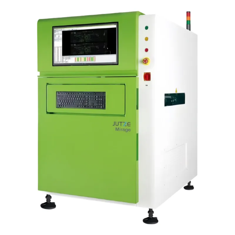
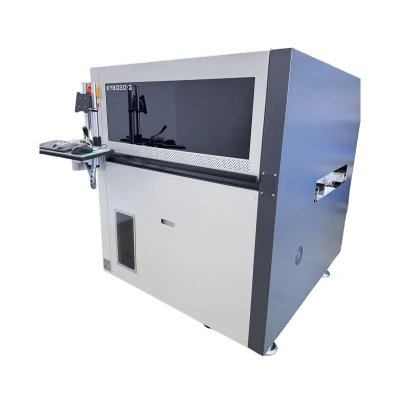
Solder Paste Inspection in Electronics Manufacturing
SPI (Solder Paste Inspection) plays a crucial role in modern electronics manufacturing, particularly on SMT (Surface Mount Technology) production lines. Its importance is primarily reflected in the following aspects:
Ensuring Solder Joint Quality Through Source Control
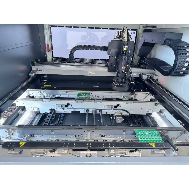
Solder paste printing is the first critical step in the SMT process, and its quality directly determines the soldering results of the subsequent reflow process. SPI uses 3D optical technologies (such as structured light, confocal, or stereo vision) to perform a comprehensive inspection of the solder paste, detecting defects such as volume, area, height, misalignment, bridging, insufficient solder, excess solder, and collapse. This ensures that “problems are caught at the printing station,” intercepting defects at the source and preventing them from entering downstream processes, which could lead to batch rework or product failure.
Improving First-Pass Yield (FPY) and Reducing Rework Costs
Statistics show that approximately 70% of SMT soldering defects stem from poor solder paste printing. SPI’s early identification and feedback of abnormal printing parameters (such as squeegee pressure, speed, release speed, and stencil cleanliness), combined with SPC (Statistical Process Control), can significantly improve first-piece yield and overall line first-pass yield, while drastically reducing labor hours and material waste caused by AOI false positives, X-ray re-inspection, and manual rework.
Supporting Process Optimization and Data Traceability
SPI provides quantifiable 3D data (such as solder paste volume deviation of ±10% and height CV values), offering objective evidence for stencil design verification, printing parameter optimization, and the introduction of new materials (such as fine-pitch or lead-free solder paste). It also generates a complete inspection report for each PCB, meeting the traceability requirements for critical processes specified in standards such as IPC-610, IATF 16949, ISO 13485, and other standards regarding traceability requirements for critical processes.
Adapting to High-Density and Miniaturization Trends
With the widespread adoption of components such as 01005, 0.3mm pitch CSP, FCCSP, and Mini LED, traditional visual inspection or 2D AOI can no longer accurately assess solder paste morphology on micro-pads. The SPI’s sub-micron Z-axis resolution and high-precision 3D reconstruction capabilities make it an indispensable quality control tool for the mass production of advanced packaging and high-reliability products (such as automotive electronics and medical devices).
Empowering Smart Manufacturing and Closed-Loop Feedback
High-end SPI systems can be integrated with MES, SPC platforms, and printers (such as DEK and MPM) to achieve closed-loop control (“inspection → analysis → automatic compensation → reprinting”), driving the upgrade of SMT production lines toward automation, digitization, and self-optimization.